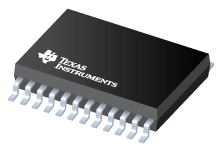
Datasheet Texas Instruments TPS65105PWPG4 — Ficha de datos
| Fabricante | Texas Instruments |
| Serie | TPS65105 |
| Numero de parte | TPS65105PWPG4 |

4-CH LCD Bias w / Totalmente Int.
Hojas de datos
TPS6510x Triple Output LCD Supply With Linear Regulator and VCOM Buffer datasheet
PDF, 1.7 Mb, Revisión: D, Archivo publicado: agosto 31, 2016
Extracto del documento
Precios
Descripción detallada
Pos. Bomba de carga, 3.3V LDO Contr., 0.96A Min. Boost Ilim, Fault y VCOM 24-HTSSOP -40 a 85
Estado
| Estado del ciclo de vida | Activo (Recomendado para nuevos diseños) |
| Disponibilidad de muestra del fabricante | No |
Embalaje
| Pin | 24 |
| Package Type | PWP |
| Industry STD Term | HTSSOP |
| JEDEC Code | R-PDSO-G |
| Package QTY | 60 |
| Carrier | TUBE |
| Device Marking | TPS65105 |
| Width (mm) | 4.4 |
| Length (mm) | 7.8 |
| Thickness (mm) | 1 |
| Pitch (mm) | .65 |
| Max Height (mm) | 1.2 |
| Mechanical Data | Descargar |
Paramétricos
| DisplayType | LCD Unipolar |
| IC Integration | LCD Bias |
| Level Shifter/Scan Driver | N/A Ch |
| Pin/Package | 24HTSSOP, 24VQFN |
| Source Driver Voltage(Max) | 15 V |
| Source Driver Voltage(Min) | 5 V |
| Special Function | VCOM/OpAmp |
| Target Application | 7 inches or less,7 to 13 inches |
| Vin(Max) | 5.8 V |
| Vin(Min) | 2.7 V |
Plan ecológico
| RoHS | Obediente |
Kits de diseño y Módulos de evaluación
- Evaluation Modules & Boards: TPS65140EVM-031
TPS65140 Evaluation Module
Estado del ciclo de vida: Activo (Recomendado para nuevos diseños) - Evaluation Modules & Boards: TPS65100EVM-030
TPS65100 Evaluation Module
Estado del ciclo de vida: Activo (Recomendado para nuevos diseños)
Notas de aplicación
- Load Disconnect for the TPS6510x (Rev. A)PDF, 69 Kb, Revisión: A, Archivo publicado: feb 8, 2017
Many boost converters have an external rectifier diode. The input voltage of the TPS6510x main boostconverter is connected to the output voltage when the device is disabled. Due to the direct pass from theinput to the output, the converter has no short-circuit protection. This application report describes how touse a PNP transistor and some passive components to disconnect the boost converte - Customizing your TPS6510x/TPS6514XPDF, 233 Kb, Archivo publicado: jun 22, 2004
This application report shows how to use external circuitry to boost the output voltage capability of the positive and negative charge pumps of the TPS6510x and TPS6514x triple output power supplies. In addition the report shows how to use external circuitry to modify the internally controlled sequencing implement sequencing delay and short circuit protection. - How to Compensate the TPS6510x and the TPS6514xPDF, 1.1 Mb, Archivo publicado: agosto 30, 2016
The boost converters in the TPS6510x (TPS65100 TPS65101 TPS65105) and the TPS6514x (TPS65140 TPS65141 TPS65145) series use external loop compensation providing high flexibility in LCD supply design. If designing a typical application scheme use the recommended components from the TPS6510x datasheet (SLVS496) and the TPS6514x datasheet (SLVS497). This application note gives a deeper understand - Basic Calculation of an Inverting Buck-Boost Power Stage (Rev. A)PDF, 431 Kb, Revisión: A, Archivo publicado: agosto 28, 2017
This application note provides basic formulas that you need to design the power stage of an invertingbuck-boost converter. The premise is that the power switch is integrated in the IC and the rectification isdone by a diode (non-synchronous power stage). It provides all the formulas and considerations that youneed to select the external power components such as the inductor the diode and t - Generation of a VCOM buffer input using PWM signalPDF, 439 Kb, Archivo publicado: dic 21, 2015
In an LCD the backlight shines through the liquid crystal material and the voltage across the liquid crystal controls how much light shines through it. An active matrix LCD (AMLCD) contains many pixels arranged in a grid pattern. The voltage across each pixel is controlled individually so that high resolution images can be created. One terminal of every pixel is connected to a common plane. The v - Understanding Undervoltage Lockout in Power Devices (Rev. A)PDF, 90 Kb, Revisión: A, Archivo publicado: sept 19, 2018
Many integrated circuits include an undervoltage lockout (UVLO) function to disable the device at low supply voltages. Below the minimum supply voltage the function and performance of a device may be undefined making it impossible to predict system behavior. This application note explains how to correctly understand the undervoltage lockout specification in the data sheets of TI's power products. - Minimizing Ringing at the Switch Node of a Boost ConverterPDF, 201 Kb, Archivo publicado: sept 15, 2006
The application report explains how to use proper board layout and/or a snubber to reduce high-frequency ringing at the switch node of a boost converter. - Basic Calculation of a Boost Converter's Power Stage (Rev. C)PDF, 186 Kb, Revisión: C, Archivo publicado: enero 8, 2014
This application note gives the equations to calculate the power stage of a boost converter built with an IC with integrated switch and operating in continuous conduction mode. It is not intended to give details on the functionality of a boost converter (see Reference 1) or how to compensate a converter. See the references at the end of this document if more detail is needed.
Linea modelo
Serie: TPS65105 (5)
- TPS65105PWP TPS65105PWPG4 TPS65105PWPR TPS65105RGER TPS65105RGERG4
Clasificación del fabricante
- Semiconductors > Power Management > LCD/OLED Display Bias Solutions