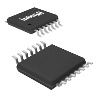
Plastic Packages for Integrated Circuits
Thin Shrink Small Outline Exposed Pad Plastic Packages (EPTSSOP)
N M38.173B INDEX
AREA E 0.25(0.010) M E1 2 38 LEAD THIN SHRINK SMALL OUTLINE PLASTIC PACKAGE
INCHES GAUGE
PLANE -B1 B M SYMBOL
A 3
TOP VIEW 0.25
0.010 0.05(0.002)
-A-L SEATING PLANE
A D О± -C-A2
c e A1 b
0.10(0.004) M 0.10(0.004)
C A M 2 -3 MIN MAX NOTES 0.047 -1.20 -0.002 0.006 0.05 0.15 -A2 0.031 0.051 0.80 1.05 -b 0.0075 0.0106 0.17 0.27 9 c 0.0035 0.0079 0.09 0.20 -D 0.378 0.386 9.60 9.80 3 E1 0.169 0.177 4.30 4.50 4 e 0.0197 BSC 0.500 BSC -E 0.246 0.256 6.25 6.50 -L 0.0177 0.0295 0.45 0.75 6 8o 0o N B S MILLIMETERS MAX A1 О±
1 MIN 38
0o 38 7
8o -P -0.256 -6.5 11 P1 -0.126 -3.2 11
Rev. 0 9/06 P1 NOTES:
1. These package dimensions are within allowable dimensions of
JEDEC MO-153-BD-1, Issue F. N 2. Dimensioning and tolerancing per ANSI Y14.5M-1982. P 3. Dimension “D” does not include mold flash, protrusions or gate
burrs. Mold flash, protrusion and gate burrs shall not exceed
0.15mm (0.006 inch) per side. BOTTOM VIEW 4. Dimension “E1” does not include interlead flash or protrusions.
Interlead flash and protrusions shall not exceed 0.15mm (0.006 …
