Datasheet Texas Instruments 74AC11240 — Ficha de datos
| Fabricante | Texas Instruments |
| Serie | 74AC11240 |
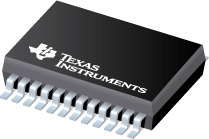
Buffers / controladores octales
Hojas de datos
Octal Buffer/Line Driver With 3-State Outputs datasheet
PDF, 573 Kb, Revisión: A, Archivo publicado: abr 1, 1996
Extracto del documento
Precios
Estado
| 74AC11240DBLE | 74AC11240DBR | 74AC11240DBRG4 | 74AC11240DW | 74AC11240PW | |
|---|---|---|---|---|---|
| Estado del ciclo de vida | Obsoleto (El fabricante ha interrumpido la producción del dispositivo) | Activo (Recomendado para nuevos diseños) | Activo (Recomendado para nuevos diseños) | Activo (Recomendado para nuevos diseños) | Activo (Recomendado para nuevos diseños) |
| Disponibilidad de muestra del fabricante | No | No | No | No | No |
Embalaje
| 74AC11240DBLE | 74AC11240DBR | 74AC11240DBRG4 | 74AC11240DW | 74AC11240PW | |
|---|---|---|---|---|---|
| N | 1 | 2 | 3 | 4 | 5 |
| Pin | 24 | 24 | 24 | 24 | 24 |
| Package Type | DB | DB | DB | DW | PW |
| Industry STD Term | SSOP | SSOP | SSOP | SOIC | TSSOP |
| JEDEC Code | R-PDSO-G | R-PDSO-G | R-PDSO-G | R-PDSO-G | R-PDSO-G |
| Width (mm) | 5.3 | 5.3 | 5.3 | 7.5 | 4.4 |
| Length (mm) | 8.2 | 8.2 | 8.2 | 15.4 | 7.8 |
| Thickness (mm) | 1.95 | 1.95 | 1.95 | 2.35 | 1 |
| Pitch (mm) | .65 | .65 | .65 | 1.27 | .65 |
| Max Height (mm) | 2 | 2 | 2 | 2.65 | 1.2 |
| Mechanical Data | Descargar | Descargar | Descargar | Descargar | Descargar |
| Package QTY | 2000 | 2000 | 25 | 60 | |
| Carrier | LARGE T&R | LARGE T&R | TUBE | TUBE | |
| Device Marking | AE240 | AE240 | AC11240 | AE240 |
Paramétricos
| Parameters / Models | 74AC11240DBLE | 74AC11240DBR | 74AC11240DBRG4 | 74AC11240DW | 74AC11240PW |
|---|---|---|---|---|---|
| Approx. Price (US$) | 1.65 | 1ku | ||||
| Bits | 8 | 8 | 8 | 8 | |
| Bits(#) | 8 | ||||
| F @ Nom Voltage(Max), Mhz | 100 | 100 | 100 | 100 | |
| F @ Nom Voltage(Max)(Mhz) | 100 | ||||
| ICC @ Nom Voltage(Max), mA | 0.08 | 0.08 | 0.08 | 0.08 | |
| ICC @ Nom Voltage(Max)(mA) | 0.08 | ||||
| Input Type | CMOS | ||||
| Operating Temperature Range, C | -40 to 85 | -40 to 85 | -40 to 85 | -40 to 85 | |
| Operating Temperature Range(C) | -40 to 85 | ||||
| Output Drive (IOL/IOH)(Max), mA | -24/24 | -24/24 | -24/24 | -24/24 | |
| Output Drive (IOL/IOH)(Max)(mA) | -24/24 | ||||
| Output Type | CMOS | ||||
| Package Group | SSOP | SSOP | SSOP | SOIC | TSSOP |
| Package Size: mm2:W x L, PKG | 24SSOP: 64 mm2: 7.8 x 8.2(SSOP) | 24SSOP: 64 mm2: 7.8 x 8.2(SSOP) | 24SOIC: 160 mm2: 10.3 x 15.5(SOIC) | 24TSSOP: 50 mm2: 6.4 x 7.8(TSSOP) | |
| Package Size: mm2:W x L (PKG) | See datasheet (PDIP) | ||||
| Rating | Catalog | Catalog | Catalog | Catalog | Catalog |
| Schmitt Trigger | No | No | No | No | No |
| Technology Family | AC | AC | AC | AC | AC |
| VCC(Max), V | 5.5 | 5.5 | 5.5 | 5.5 | |
| VCC(Max)(V) | 5.5 | ||||
| VCC(Min), V | 3 | 3 | 3 | 3 | |
| VCC(Min)(V) | 3 | ||||
| Voltage(Nom), V | 3.3,5 | 3.3,5 | 3.3,5 | 3.3,5 | |
| Voltage(Nom)(V) | 3.3 5 | ||||
| tpd @ Nom Voltage(Max), ns | 11.7,8.4 | 11.7,8.4 | 11.7,8.4 | 11.7,8.4 | |
| tpd @ Nom Voltage(Max)(ns) | 11.7 8.4 |
Plan ecológico
| 74AC11240DBLE | 74AC11240DBR | 74AC11240DBRG4 | 74AC11240DW | 74AC11240PW | |
|---|---|---|---|---|---|
| RoHS | Desobediente | Obediente | Obediente | Obediente | Obediente |
| Pb gratis | No |
Notas de aplicación
- Live InsertionPDF, 150 Kb, Archivo publicado: oct 1, 1996
Many applications require the ability to exchange modules in electronic systems without removing the supply voltage from the module (live insertion). For example an electronic telephone exchange must always remain operational even during module maintenance and repair. To avoid damaging components additional circuitry modifications are necessary. This document describes in detail the phenomena tha - Introduction to LogicPDF, 93 Kb, Archivo publicado: abr 30, 2015
- Shelf-Life Evaluation of Lead-Free Component FinishesPDF, 1.3 Mb, Archivo publicado: mayo 24, 2004
The integrated circuit (IC) industry is converting to lead (Pb)-free termination finishes for leadframe-based packages. IC component users need to know the maximum length of time that components can be stored prior to being soldered. This study predicts shelf life of the primary Pb-free finishes being proposed by the industry. Components were exposed to a controlled environment, with known aging a - Semiconductor Packing Material Electrostatic Discharge (ESD) ProtectionPDF, 337 Kb, Archivo publicado: jul 8, 2004
Forty-eight-pin TSSOP components that were packaged using Texas Instruments (TI) standard packing methodology were subjected to electrical discharges between 0.5 and 20 kV as generated by an IEC ESD simulator to determine the level of ISD protection provided by the packing materials. The testing included trays tape and reel and magazines. Additional units were subjected to the same discharge - Understanding and Interpreting Standard-Logic Data Sheets (Rev. C)PDF, 614 Kb, Revisión: C, Archivo publicado: dic 2, 2015
- Input and Output Characteristics of Digital Integrated CircuitsPDF, 1.7 Mb, Archivo publicado: oct 1, 1996
This report contains a comprehensive collection of the input and output characteristic curves of typical integrated circuits from various logic families. These curves go beyond the information given in data sheets by providing additional details regarding the characteristics of the components. This knowledge is particularly useful when for example a decision must be made as to which circuit shou - CMOS Power Consumption and CPD Calculation (Rev. B)PDF, 89 Kb, Revisión: B, Archivo publicado: jun 1, 1997
Reduction of power consumption makes a device more reliable. The need for devices that consume a minimum amount of power was a major driving force behind the development of CMOS technologies. As a result CMOS devices are best known for low power consumption. However for minimizing the power requirements of a board or a system simply knowing that CMOS devices may use less power than equivale - TI IBIS File Creation Validation and Distribution ProcessesPDF, 380 Kb, Archivo publicado: agosto 29, 2002
The Input/Output Buffer Information Specification (IBIS) also known as ANSI/EIA-656 has become widely accepted among electronic design automation (EDA) vendors semiconductor vendors and system designers as the format for digital electrical interface data. Because IBIS models do not reveal proprietary internal processes or architectural information semiconductor vendors? support for IBIS con - Implications of Slow or Floating CMOS Inputs (Rev. D)PDF, 260 Kb, Revisión: D, Archivo publicado: jun 23, 2016
- Designing With Logic (Rev. C)PDF, 186 Kb, Revisión: C, Archivo publicado: jun 1, 1997
Data sheets which usually give information on device behavior only under recommended operating conditions may only partially answer engineering questions that arise during the development of systems using logic devices. However information is frequently needed regarding the behavior of the device outside the conditions in the data sheet. Such questions might be:?How does a bus driver behave w - Using High Speed CMOS and Advanced CMOS in Systems With Multiple VccPDF, 43 Kb, Archivo publicado: abr 1, 1996
Though low power consumption is a feature of CMOS devices sometimes this feature does not meet a designer?s system power supply constraints. Therefore a partial system power down or multiple Vcc supplies are used to meet the needs of the system. This document shows electrostatic discharge protection circuits. It also provides circuit and bus driver examples of partial system power down and curren
Linea modelo
Serie: 74AC11240 (5)
Clasificación del fabricante
- Semiconductors> Logic> Buffer/Driver/Transceiver> Inverting Buffer/Driver