PDF, 748 Kb, Revisión: A, Archivo publicado: jun 12, 2014
Extracto del documento
Product
Folder Sample &
Buy Support &
Community Tools &
Software Technical
Documents CSD75207W15
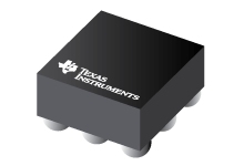
SLPS418A – JUNE 2013 – REVISED JUNE 2014 CSD75207W15 Dual P-Channel NexFET™ Power MOSFET
1 Features 1 Dual P-Channel MOSFETs
Common Source Configuration
Small Footprint 1.5-mm Г— 1.5-mm
Gate-Source Voltage Clamp
Gate ESD Protection >4 kV
– HBM JEDEC standard JESD22-A114
Pb and Halogen Free
RoHS Compliant Product Summary
TA = 25°C UNIT Drain-to-Drain Voltage –20 V Qg Gate Charge Total (–4.5 V) 2.9 nC Qgd Gate Charge Gate to Drain RD1D2(on) Drain-to-Drain On Resistance
VGS(th) 0.4 nC VGS = –1.8 V 119 mΩ VGS = –2.5 V 64 mΩ VGS = –4.5 V 45 mΩ Threshold Voltage –0.8 V Ordering Information(1) 2 Applications TYPICAL VALUE VD1D2 Battery Management
Battery Protection
Load and Input Switching Device Package Media CSD75207W15 1.5-mm Г— 1.5-mm
Wafer Level Package 7-Inch
Reel Qty Ship 3000 Tape and
Reel (1) For all available packages, see the orderable addendum at
the end of the data sheet. 3 Description Absolute Maximum Ratings The CSD75207W15 device is designed to deliver the …
