Sample &
Buy Product
Folder Support &
Community Tools &
Software Technical
Documents CSD17552Q3A
SLPS387B – SEPTEMBER 2012 – REVISED JANUARY 2016 CSD17552Q3A 30 V N-Channel NexFET™ Power MOSFETs
1 Features 1 Product Summary Ultra-Low Qg and Qgd
Low Thermal Resistance
Avalanche Rated
Pb Free
RoHS Compliant
Halogen Free
SON 3.3 mm Г— 3.3 mm Plastic Package TA = 25В°C TYPICAL VALUE Drain-to-Source Voltage 30 V Qg Gate Charge Total (4.5 V) 9.0 nC Qgd Gate Charge Gate-to-Drain RDS(on) Drain-to-Source On Resistance VGS(th) Threshold Voltage Point-of-Load Synchronous Buck in Networking,
Telecom, and Computing Systems
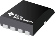
Optimized for Control FET Applications This 30 V, 5.5 mО©, 3.3 mm Г— 3.3 mm SON
NexFETв„ў power MOSFET is designed to minimize
losses in power conversion applications. S VGS = 10 V 5.5 mΩ 1.5 V DEVICE QTY MEDIA PACKAGE SHIP CSD17552Q3A 2500 13-Inch Reel CSD17552Q3AT 250 7-Inch Reel SON
3.3 mm Г— 3.3 mm
Plastic Package Tape and
Reel 8 1 7 2 6 3 5 4 Absolute Maximum Ratings
VALUE UNIT Drain-to-Source Voltage 30 V VGS Gate-to-Source Voltage В±20 V Continuous Drain Current, TC = 25В°C 60 TA = 25В°C unless otherwise stated A Continuous Drain Current, Silicon Limited 74 A Continuous Drain Current, TA = 25В°C(1) 15 A IDM Pulsed Drain Current, TA = 25В°C(2) 84 A PD Power Dissipation(1) 2.6 W D TJ,
Tstg Operating Junction Temperature, …
